When we talk about an international company always Competition is the word that sets in everybody’s mind. The two great company Samsung and TSMC is fighting with a new product to have the market in their hand. In a recent interview, Samsung officials stated that manufacturers had already started producing the 3nm GAAFET chips.
The size of the product is really hard to find in the advertisements and it’s hard to compare both the leading companies at this point. Samsung had already started their celebration process regarding their new achievement of producing the first GAAFET 3 nanometer chips.
Reports and studies have claimed that The 3nm punch can beat the TSMC quite easily. Modern Success doesn’t mean that Samsung is going to give better performance regarding the process of Thermals. At the same time, this is also true that Samsung was able to open the door.
In the past few months, it was quite evident that TSMC was only giving the road maps for achieving success. The officials of TSMC very recently claimed that they were planning for 5 different 3nm processes.
Reports and Studies have claimed that TSMC is all ready and is going into production for the 3nm Chips within the next few months. The market availability is all set and might get released in early 2023. Samsung on the other hand uses its semiconductor to produce its own 3nm chips.
Past History has already claimed that the Samsung Nods have been quite behind that TSMC’s advertised size of the chips. Histories don’t matter nowadays and the success that happened a couple of years can’t be drawn now. The modernization in the technologies used has impacted the uses of Chip as well.
Samsung GAAFET technology provides 45% of improved power consumption. Increased performance as well by 23% and it takes 16% reduced area as well. This process is better as compared to 5nm nodes. 3nm process for the second generation is also in the mix of the plan for the brand Samsung.
The second-generation process reduces power consumption by a minimum of 50%. 30% improved in performance as well. Its area consumption is also reduced by 35% which is also a huge advantage.
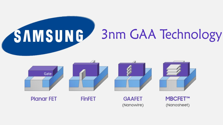
The full form of GGA stands for Gate All Around”. This stands for the complete introduction of new technology into the market. This process also develops a huge amount of channel density. “FinFET” is the term that is used for the process of Evolution. Better Performance, and reduction in power consumption all depend on how we are going to use them.
TSMC has no plans of jumping into the GAAFET, they are having plans for producing 2nm nodes which are expected to be in production for 2024.
“Always stay updated with us and visit GeeksULTD for real-time updates.”


